Researchers demonstrate 40-channel optical communication link
About Optica
09 June 2022
Researchers demonstrate 40-channel optical communication link
Silicon-based device could help meet ever-growing need to move more data faster
WASHINGTON — Researchers have demonstrated a silicon-based optical communication link that combines two multiplexing technologies to create 40 optical data channels that can simultaneously move data. The new chip-scale optical interconnect can transmit about 400 GB of data per second — the equivalent of about 100,000 streaming movies. This could improve data-intensive internet applications from video streaming services to high-capacity transactions for the stock market.

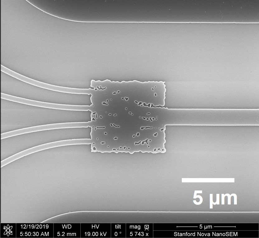
Caption: The researchers designed and optimized a mode-division multiplexer that transforms each of the 10 wavelengths into four new beams that each have different shapes. This fourfold increase in data capacity creates 40 channels.
Image Credit: Kiyoul Yang, Stanford University
“As demands to move more information across the internet continue to grow, we need new technologies to push data rates further,” said Peter Delfyett, who led the University of Central Florida College of Optics and Photonics (CREOL) research team. “Because optical interconnects can move more data than their electronic counterparts, our work could enable better and faster data processing in the data centers that form the backbone of the internet.”
A multi-institutional group of researchers describes the new optical communication link in the Optica Publishing Group journal Optics Letters. It achieves 40 channels by combining a frequency comb light source based on a new photonic crystal resonator developed by the National Institute of Standards and Technology (NIST) with an optimized mode-division multiplexer designed by the researchers at Stanford University. Each channel can be used to carry information much like different stereo channels, or frequencies, transmit different music stations.
“We show that these new frequency combs can be used in fully integrated optical interconnects,” said Chinmay Shirpurkar, co-first author of the paper. “All the photonic components were made from silicon-based material, which demonstrates the potential for making optical information handling devices from low-cost, easy-to-manufacture optical interconnects.”
In addition to improving internet data transmission, the new technology could also be used to make faster optical computers that could provide the high levels of computing power needed for artificial intelligence, machine learning, large-scale emulation and other applications.
Using multiple light dimensions
The new work involved research teams led by Firooz Aflatouni of the University of Pennsylvania, Scott B. Papp from NIST, Jelena Vuckovic from Stanford University and Delfyett from CREOL. It is part of the DARPA Photonics in the Package for Extreme Scalability (PIPES) program, which aims to use light to vastly improve the digital connectivity of packaged integrated circuits using microcomb-based light sources.

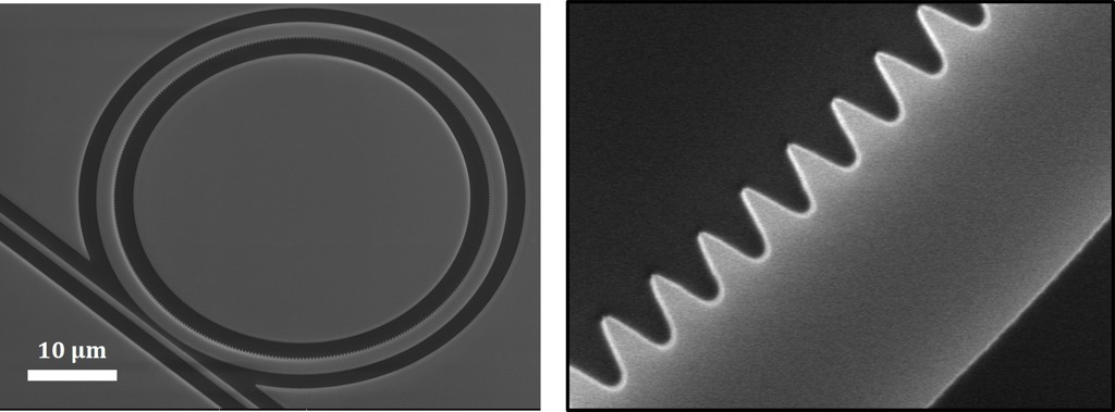
Caption: Researchers demonstrated a silicon-based optical communication link that combines two multiplexing technologies to create 40 optical data channels. The ring-shaped photonic crystal resonator (left) features a nanopattern inside (right) that splits a selected resonant mode for comb generation. Images taken with scanning electron microscopy
Image Credit:Su-Peng Yu, NIST
The researchers created the optical link using tantalum pentoxide (Ta2O5) waveguides on a silicon substrate fabricated into a ring with a nanopatterned oscillation on the inner wall. The resulting photonic crystal micro-ring resonator turns a laser input into ten different wavelengths. They also designed and optimized a mode-division multiplexer that transforms each wavelength into four new beams that each have different shapes. Adding this spatial dimension enables a fourfold increase in data capacity, creating the 40 channels.
Once the data is encoded onto each beam shape and each beam color, the light is recombined back into a single beam and transmitted to its destination. At the final destination, the wavelengths and beam shapes are separated so that each channel can be received and detected independently, without interference from the other transmitted channels.
“An advantage of our link is that the photonic crystal resonator enables easier soliton generation and a flatter comb spectrum than those demonstrated with conventional ring resonators,” said co-first author Jizhao Zang from NIST. “These features are beneficial for optical data links.”
Better performance with inverse design
To optimize the mode division multiplexer, the researchers used a computational nanophotonic design approach called photonic inverse-design. This method provides a more efficient way to explore a full range of possible designs while offering smaller footprints, better efficiencies and new functionalities.
“The photonic inverse-design approach makes our link highly customizable to meet the needs of specific applications,” said co-first author Kiyoul Yang from Stanford University.
Tests of the new device matched well with simulations and showed that the channels exhibited a low crosstalk of less than -20 dB. Using less than −10 dBm of received optical receiver power, the link performed error-free data transmission in 34 out of the 40 channels using a PRBS31 pattern, a standard used to test high-speed circuits under stress.
The researchers are now working to further improve the device by incorporating photonic crystal micro-ring resonators that produce more wavelengths or by using more complex beam shapes. Commercializing these devices would require the full integration of a transmitter and receiver chip with high bandwidth, low power consumption and a small footprint. This could enable the next generation of optical interconnects for use in data-center networks.
Open-source code for the photonic optimization software used in the paper is available at https://github.com/stanfordnqp/spins-b.
Paper: C. Shirpurkar, J. Zang, K. Y. Yang, D. Carlson, S. P. Yu, E. Lucas, S.V. Pericherla, J. Yang, M. Guidry, D. Lukin, G.H. Ahn, J. Lu, L. Trask, F. Aflatouni, J. Vuĉkovic, S. B. Papp, P. J. Delfyett, “Photonic crystal resonators for inverse-designed multi-dimensional optical interconnects,” Opt. Lett., 47, 12 (2022).
DOI: 10.1364/OL.461272
About Optica Publishing Group
Optica Publishing Group is a division of the society, Optica, Advancing Optics and Photonics Worldwide. It publishes the largest collection of peer-reviewed and most-cited content in optics and photonics, including 18 prestigious journals, the society’s flagship member magazine, and papers and videos from more than 835 conferences. With over 400,000 journal articles, conference papers and videos to search, discover and access, our publications portfolio represents the full range of research in the field from around the globe.
About Optics Letters
Optics Letters has been publishing high-impact research in the field of photonics for over 45 years and offers rapid dissemination of new results in all areas of optical science with short, original, peer-reviewed communications. Optics Letters accepts papers that are noteworthy to a substantial part of the optics community. Published by Optica Publishing Group and led by Editor-in-Chief Miguel Alonso, Institut Fresnel, École Centrale de Marseille and Aix-Marseille Université, France, University of Rochester, USA. For more information, visit Optics Letters.
Media Contact
